
Story
SK Hynix Breaks Ground on $4 Billion Indiana AI Chip Packaging Plant
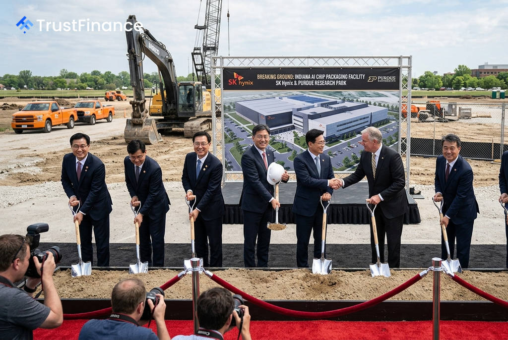
South Korean chipmaker SK Hynix on Thursday held a groundbreaking ceremony for its advanced semiconductor packaging and research facility in West Lafayette, Indiana. The project represents an investment of more than $4 billion and is a significant step in expanding the company's U.S. footprint to meet surging demand for memory chips essential for artificial intelligence applications.
Facility Details and Strategic Goals
The new site, located at the Purdue Research Park, will house a next-generation high-bandwidth memory (HBM) packaging line and an AI semiconductor research and development center. According to company statements, the facility is scheduled to begin cleanroom operations in the second half of 2028.
This investment is strategically designed to bring SK Hynix's advanced packaging capabilities closer to major U.S. customers like Nvidia, Microsoft, and Google. The project is also expected to foster local engineering talent through ties with Purdue University and create approximately 7,000 direct and indirect jobs, bolstering the regional economy and the U.S. semiconductor supply chain.
Riding the AI-Driven HBM Wave
Demand for HBM has exploded as technology companies race to build out AI data centers. HBM is a specialized memory that stacks chips vertically, enabling faster data processing and lower power consumption, which is critical for the intensive computing required by AI models.
 Ad
SK Hynix is a dominant force in this market, accounting for 58% of global HBM revenue in the first quarter of 2026, according to Counterpoint Research. The Indiana facility will add crucial U.S.-based capacity at a time when memory availability is a key constraint on the expansion of AI infrastructure, a trend underscored by strong revenue forecasts from major customers like Nvidia.
Government Support and Investment Context
The project is backed by significant U.S. government support under the CHIPS Act. In December 2024, the government finalized $458 million in grants and up to $500 million in loans for the facility.
SK Hynix first announced an investment agreement with Indiana officials in 2024, initially valued at $3.87 billion, which has since increased to over $4 billion. This U.S. expansion is part of a broader global investment strategy by the company, which recently approved approximately 54.3 trillion won (about $38.30 billion) for investments through 2031, including for its chip fabrication plants in South Korea.
Read next
More on Stocks
FTC Orders Walmart, Uber, Delta to Disclose Data on Personalized Pricing
The U.S. Federal Trade Commission is demanding nine major companies, including leading retail, travel, and gig economy firms, to provide information on how they use consumer data for setting individual prices and wages.

Google Launches Gemini 4 Carbon AI Model to Bolster Cybersecurity Capabilities
Alphabet's Google has unveiled Gemini 4 Carbon, its latest AI model specifically designed for advanced cybersecurity tasks like vulnerability detection and secure code generation. The launch escalates competition with rivals OpenAI and Anthropic in the enterprise AI market.

Oracle Shares Surge After Unveiling $225 Billion Revenue Target for 2030
Oracle stock rose sharply after the company presented a long-term financial outlook targeting at least $225 billion in annual revenue by fiscal 2030, driven by its expanding AI infrastructure business.
DOJ Scrutinizes Nvidia's $12.9B Hugging Face Deal Amid Broader Antitrust Probe, Sources Say
The U.S. Department of Justice is reportedly examining Nvidia's planned $12.93 billion acquisition of AI platform Hugging Face as part of a wider, ongoing antitrust investigation into the chipmaker's market conduct.